What is Scanning Electron Microscope (SEM)?
Scanning Electron Microscope (SEM) is a device for obtaining a three-dimensional surface of a sample by an electron beam onto the surface of a sample.
scanning electron microscopy (SEM) method, not being a destructive method, allows you to quickly carry out quantitative morphological analysis and measurement of the linear dimensions of the surface of solid-state structures with a resolution of up to one nanometer (equal to 1 x 10⁻⁶ mm).
The use of a field emission source for the formation of a diagnostic beam allows scanning electron microscopy to visualize the heterogeneity of the structure within one monolayer, to analyze the chemical composition of the surface using the built-in energy dispersion analysis (EDS) unit, to determine the electrical activity of defects using the induced current technique, etc.
Simultaneous analysis using energy-dispersive spectroscopy (EDS) in a scanning electron microscope can reveal which elements are composed of in a relatively short time.
how Scanning Electron Microscope works?
An electron probe (electron beam) is directed to the analyzed sample. As a result of the interaction between the electron probe and the sample, low-energy secondary electrons are generated, which are collected by the secondary electron detector.

The intensity of the detector’s electrical signal depends both on the nature of the sample (to a lesser extent) and on the topography (to a greater extent) of the sample in the field of interaction.

Thus, by scanning the surface of the object with an electron beam, it is possible to obtain a map of the surface of the analyzed zone.
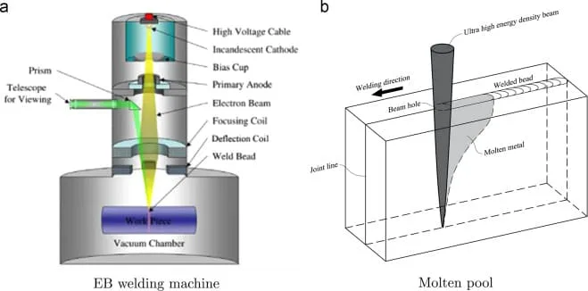
A narrow electron probe is generated by an electron gun, which plays the role of a source of electrons, and is focused by electron lenses (usually electromagnetic, sometimes electrostatic).
Scanning coils deflect the probe in two mutually perpendicular directions, scanning the surface of the sample with a probe, similar to scanning the screen of a cathode ray tube with an electron beam of a television. The source of electrons, electron lenses (usually toroidal magnetic) and deflection coils form a system called an electron column.
Scanning Electron Microscope Configuration
The SEM consists of an electron gun that generates and accelerates an electron beam, a focusing lens and objective lens that finely collects the electron beam, and a deflection coil that adjusts the path of the electron beam until the electron leaving the filament touches the specimen.
A sample stage for moving specimens is located in the vacuum barrel at the bottom of the column, and various detectors such as secondary electron detectors can be attached to the barrel.
The lower part of the equipment consists of a vacuum pump that keeps the vacuum chamber below 10‐5torr, a high-voltage supply device that supplies high voltage to electron guns and detectors, electronics that control the entire system or process the collected signals, and an isolation stand those blocks vibrations transmitted to the equipment from the outside.
Applications of SEM
The application of electron microscopy in various branches of not only science, but also technology is characterized by the use of different microscopy.
Let’s briefly see each of them.
- Scanning probe microscopy is used to identify the morphological structure of a sample and to identify its surface using a probe (optical probe or needle) that comes into contact with the surface of the object under study.
- Scanning tunneling microscopy is one of the varieties of probe microscopy, the difference of which lies in the fact that the potential enters the needle scanning the surface of the object and a tunneling current is created, while the distance between the needle and the surface does not exceed 0.1 nm.
- Confocal laser scanning microscopy is carried out not only on the surface of the sample under study, but also on the given depth of the object under study. Thanks to this, it is possible to obtain clear information about the layer-by-layer structure of the medicines. When working with modern equipment, you can get a three-dimensional image of the object, as a result of which specialists can conduct a lot of research in the future.
Advantages and disadvantages
Scanning electron microscope has a number of advantages and advantages. The main advantages of SEM are the following:
- unlike an optical microscope, the magnification force reaches 300,000, which is ten times higher than the resolution of an optical device
- the ability to create the largest possible depth of field, while large objects can be obtained in focus clearly and smoothly
- it is possible to create high-quality photos.
But in addition to the advantages, scanning microscopy has certain drawbacks. Among them, the following are the main cons of SEM:
- a conventional scanning microscope is able to study only the object that is placed inside the camera and will be solid.
- all elements that have a low atomic mass and are below number 14 in the table are not studied, as they cannot be detected.
- the price of the cheapest microscope reaches several tens of thousands of dollars.
Given all this, we can safely say that the scanning electron microscope is a device that is able to show what optical microscopy fails to see.
Scanning electron microscope radiation safety concerns
Scanning electron microscopes (SEMs) are powerful tools for researchers in a variety of fields. However, the radiation generated by many SEMs can present safety concerns for operators and those nearby.
To ensure optimal safety, it is important to become familiar with the risks posed by SEM radiation and the steps necessary to mitigate them.
Radiation from SEMs typically consists of electrons or X-rays, both of which can be dangerous if not properly managed. The intensity of these radiations varies depending on factors such as specimen type, accelerating voltage, and stage position.
To protect against overexposure to radiation, researchers must use appropriate shielding techniques and employ precautionary practices when using an SEM. Protective eyewear should also be worn when operating any type of microscope that uses X-ray generation capabilities.


